Canon Inc. announced on January 13 that it has become the first company in the world to develop and practically implement inkjet-based adaptive planarization technology for semiconductor manufacturing. The breakthrough, which leverages Canon's expertise in nanoimprint lithography, represents a significant advancement in wafer processing that could reshape how advanced chips are manufactured. The Japanese imaging giant aims to commercialize equipment incorporating this technology by 2027.
The new technology, called inkjet-based adaptive planarization or IAP, addresses one of the most critical challenges in semiconductor manufacturing. As chips become increasingly miniaturized and three-dimensional, even slight surface irregularities on wafers can cause dimension errors and pattern misalignment that significantly impact production yields. Traditional planarization methods have struggled to keep pace with the demands of cutting-edge chip designs.
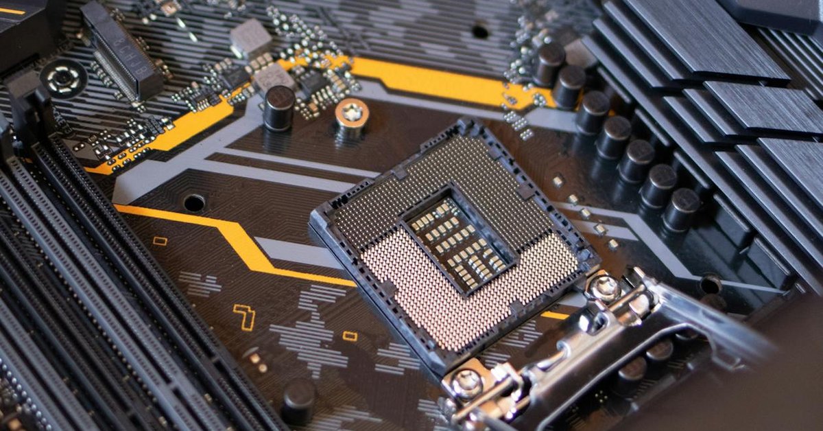
Canon's IAP system works by using an inkjet to dispense light-curable material onto wafer surfaces in a precisely tuned manner that matches the underlying topography. A flat glass plate is then pressed onto the wafer, achieving high-precision leveling across the entire 300-millimeter diameter surface in a single stamping process. This approach reduces topographical irregularity to five nanometers or less, regardless of variations in circuit design or pattern density.
The technology builds on Canon's work in nanoimprint lithography, an alternative to extreme ultraviolet lithography that has attracted attention as a potentially lower-cost method for producing advanced semiconductors. By adapting key elements of nanoimprint for planarization, Canon has developed a process that provides excellent gap fill even for high aspect ratios and delivers consistent results regardless of feature size or pattern density.
Canon and its subsidiary Canon Nanotechnologies will present their IAP research at the SPIE Advanced Lithography and Patterning Conference scheduled for February 25 at the San Jose Convention Center. The presentation will include detailed technical specifications and initial performance results that demonstrate the technology's capabilities for logic and memory device manufacturing.
The announcement comes as the semiconductor industry faces increasing pressure to develop new manufacturing techniques for next-generation chips. While Dutch company ASML dominates the market for extreme ultraviolet lithography equipment, alternatives like Canon's nanoimprint and now IAP technology offer potential pathways for chipmakers seeking to reduce costs or achieve specific manufacturing goals.
Industry analysts note that planarization is an indispensable but often overlooked step in chip fabrication. As multiple layers of films and wiring are built up during manufacturing, maintaining flat surfaces becomes increasingly challenging. Canon's ability to achieve sub-five-nanometer flatness in a single process could eliminate multiple steps from current manufacturing workflows, potentially reducing both time and cost for semiconductor producers worldwide.
Comments